- 您现在的位置:买卖IC网 > Sheet目录2011 > MAX5893EGK+D (Maxim Integrated Products)IC DAC 12BIT DUAL 500MSPS 68-QFN
MAX5893
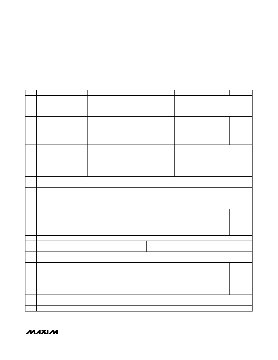
Programming Registers
Programming its registers with the SPI serial interface
sets the MAX5893 operation modes. Table 2 shows all
of the registers. The following are descriptions of each
register.
12-Bit, 500Msps Interpolating and Modulating
Dual DAC with CMOS Inputs
______________________________________________________________________________________
15
ADD
BIT 7
BIT 6
BIT 5
BIT 4
BIT 3
BIT 2
BIT 1
BIT 0
00h
Unused
0 = MSB first
1 = LSB first
Software Reset
0 = Normal
1 = Reset all
registers
Interpolator
Power-Down
0 = Normal
1 = Power-down
IDAC Power-
Down
0 = Normal
1 = Power-down
QDAC Power-
Down
0 = Normal
1 = Power-down
Unused
01h
Interpolation Rate
(Bit 7, Bit 6)
00 = No interpolation
01 = 2x interpolation
10 = 4x interpolation
11 = 8x interpolation
Third
Interpolation
Filter
Configuration
0 = Lowpass
1 = Highpass
Modulation Mode
(Bit 4, Bit 3)
00 = Modulation off
01 = fIM/2
10 = fIM/4
11 = fIM/4
Mixer Modulation
Mode
0 = Complex
1 = Real
Modulation
Sign
0 = e
-j
ω
1 = e
+j
ω
Unused
02h
0 = Two’s
complement
input data
1 = Offset
binary input
data
0 = Single
port (A),
interleaved
I/Q
1 = Dual port
I/Q input
0 = Clock output
on DATACLK
1 = Clock output
on DATACLK/B10
0 = Input data
latched on
rising clock
edge
1 = Input data
latched on falling
clock edge
0 = Data clock
input enabled
1 = Data clock
output enabled
Data
Synchronizer
0 = Enabled
1 = Disabled
Unused
03h
Unused
04h
8-Bit IDAC Fine-Gain Adjustment (see the Gain Adjustment section). Bit 7 is MSB and bit 0 is LSB. Default: 00h
05h
Unused
4-Bit IDAC Coarse-Gain Adjustment (see the Gain Adjustment
section). Bit 3 is MSB and bit 0 is LSB. Default: Fh
06h
10-Bit IDAC Offset Adjustment (see the Offset Adjustment section). Bits 7 to 0 of the 06h register are the MSB bits. Bit 1 and bit 0 are the LSB
bits in 07h register. Default: 000h
07h
IDAC IOFFSET
Direction
0 = Current on
OUTIN
1 = Current on
OUTIP
Unused
IDAC Offset
Adjustment
Bit 1
(see 06h
register)
IDAC Offset
Adjustment
Bit 0
(see 06h
register)
08h
8-Bit QDAC Fine-Gain Adjustment (see the Gain Adjustment section). Bit 7 is MSB and bit 0 is LSB. Default: 00h
09h
Unused
4-Bit QDAC Coarse-Gain Adjustment (see the Gain Adjustment
section). Bit 3 is MSB and bit 0 is LSB. Default: Fh
0Ah
10-Bit QDAC Offset Adjustment (see the Offset Adjustment section). Bits 7 to 0 of the 0Ah register are the MSB bits. Bit 1 and bit 0 are the
LSB bits in 0Bh register. Default: 000h
0Bh
QDAC
IOFFSET
Direction
0 = Current on
OUTQN
1 = Current on
OUTQP
Unused
QDAC Offset
Adjustment
Bit 1
(see 0Ah
register)
QDAC Offset
Adjustment
Bit 0
(see 0Ah
register)
0Ch
Reserved, do not write to these bits.
0Dh
Reserved, do not write to these bits.
0Eh
Reserved, do not write to these bits.
Table 2. MAX5893 Programmable Registers
Conditions in bold are default states after reset.
发布紧急采购,3分钟左右您将得到回复。
相关PDF资料
MAX5894EGK+D
IC DAC 14BIT DUAL 500MSPS 68-QFN
MAX5895EGK+D
IC DAC 16BIT 500MSPS DUAL 68-QFN
MAX5898EGK+D
IC DAC 16BIT DUAL 500MSPS 68-QFN
MAX6900ETT+T
IC RTC I2C COMPAT 6-TDFN
MAX6902ETA+T
IC RTC SPI COMPAT 8-TDFN
MAX7375AXR604+T
IC OSC SILICON SC70-3
MAX7394ATTLY+T
IC OSC SILICON 922KHZ 6-TDFN
MAX7403CSA+
IC FILTER LOWPASS 8-SOIC
相关代理商/技术参数
MAX5893EGK+TD
功能描述:数模转换器- DAC 12-Bit 2Ch 500Msps DAC RoHS:否 制造商:Texas Instruments 转换器数量:1 DAC 输出端数量:1 转换速率:2 MSPs 分辨率:16 bit 接口类型:QSPI, SPI, Serial (3-Wire, Microwire) 稳定时间:1 us 最大工作温度:+ 85 C 安装风格:SMD/SMT 封装 / 箱体:SOIC-14 封装:Tube
MAX5893EGK-D
功能描述:数模转换器- DAC RoHS:否 制造商:Texas Instruments 转换器数量:1 DAC 输出端数量:1 转换速率:2 MSPs 分辨率:16 bit 接口类型:QSPI, SPI, Serial (3-Wire, Microwire) 稳定时间:1 us 最大工作温度:+ 85 C 安装风格:SMD/SMT 封装 / 箱体:SOIC-14 封装:Tube
MAX5893EGK-TD
功能描述:数模转换器- DAC RoHS:否 制造商:Texas Instruments 转换器数量:1 DAC 输出端数量:1 转换速率:2 MSPs 分辨率:16 bit 接口类型:QSPI, SPI, Serial (3-Wire, Microwire) 稳定时间:1 us 最大工作温度:+ 85 C 安装风格:SMD/SMT 封装 / 箱体:SOIC-14 封装:Tube
MAX5893EVCMOD2
功能描述:数模转换器- DAC Evaluation Kit for the MAX5893/MAX5894/MAX5895 RoHS:否 制造商:Texas Instruments 转换器数量:1 DAC 输出端数量:1 转换速率:2 MSPs 分辨率:16 bit 接口类型:QSPI, SPI, Serial (3-Wire, Microwire) 稳定时间:1 us 最大工作温度:+ 85 C 安装风格:SMD/SMT 封装 / 箱体:SOIC-14 封装:Tube
MAX5893EVKIT
功能描述:数模转换器- DAC Evaluation Kit for the MAX5893/MAX5894/MAX5895 RoHS:否 制造商:Texas Instruments 转换器数量:1 DAC 输出端数量:1 转换速率:2 MSPs 分辨率:16 bit 接口类型:QSPI, SPI, Serial (3-Wire, Microwire) 稳定时间:1 us 最大工作温度:+ 85 C 安装风格:SMD/SMT 封装 / 箱体:SOIC-14 封装:Tube
MAX5894EGK+D
功能描述:数模转换器- DAC 14-Bit 2Ch 500Msps DAC RoHS:否 制造商:Texas Instruments 转换器数量:1 DAC 输出端数量:1 转换速率:2 MSPs 分辨率:16 bit 接口类型:QSPI, SPI, Serial (3-Wire, Microwire) 稳定时间:1 us 最大工作温度:+ 85 C 安装风格:SMD/SMT 封装 / 箱体:SOIC-14 封装:Tube
MAX5894EGK+TD
功能描述:数模转换器- DAC 14-Bit 2Ch 500Msps DAC RoHS:否 制造商:Texas Instruments 转换器数量:1 DAC 输出端数量:1 转换速率:2 MSPs 分辨率:16 bit 接口类型:QSPI, SPI, Serial (3-Wire, Microwire) 稳定时间:1 us 最大工作温度:+ 85 C 安装风格:SMD/SMT 封装 / 箱体:SOIC-14 封装:Tube
MAX5894EGK-D
功能描述:数模转换器- DAC RoHS:否 制造商:Texas Instruments 转换器数量:1 DAC 输出端数量:1 转换速率:2 MSPs 分辨率:16 bit 接口类型:QSPI, SPI, Serial (3-Wire, Microwire) 稳定时间:1 us 最大工作温度:+ 85 C 安装风格:SMD/SMT 封装 / 箱体:SOIC-14 封装:Tube